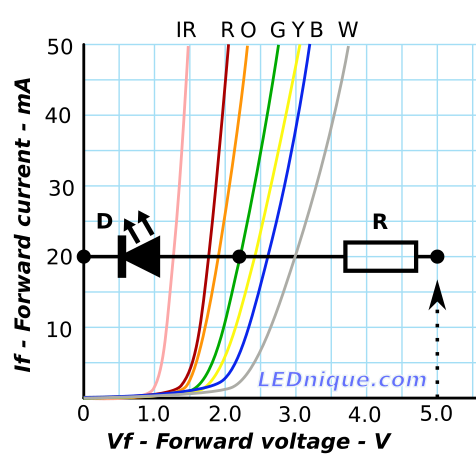
Most LED circuits require a current limiting resistor.
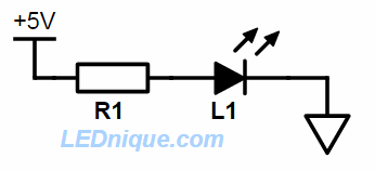
R + LED on 5 V supply.
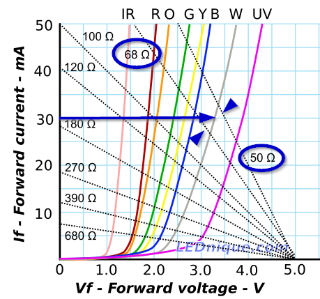
The loadline calculator makes resistor selection very simple.
Loadlines for various resistors on 5 V supply.
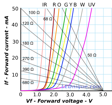
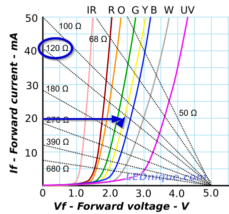
Example 1: Chose a resistor to give 20 mA on a yellow LED and 5 V supply.
Loadline for 20 mA yellow on 5 V supply.
Solution: Choose 20 mA on the If axis. Slide across to the yellow LED curve. Find the nearest loadline: in this case it’s 120 Ω.
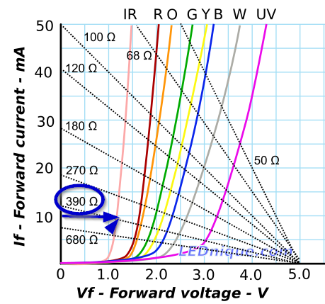
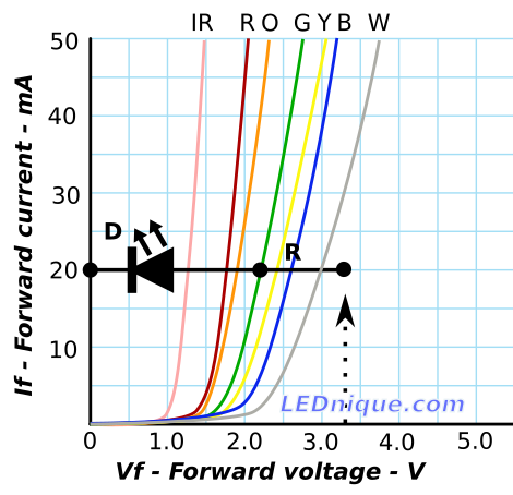
Example 2: Chose a resistor to give 10 mA on an infrared LED and 5 V supply.
Loadline 10 mA IR on 5 V supply.
Solution: Choose 10 mA on the If axis. Slide across to the IR LED curve. Find the nearest loadline: in this case it’s 390 Ω.
Example 3: Chose a resistor to give 30 mA on a white LED and 5 V supply.
Loadline 30 mA on a white LED.
Solution: Choose 30 mA on the If axis. Slide across to the white LED curve. Find the nearest loadline: in this case it’s between 50 and 68 Ω. 56 is the nearest standard value.
Not all mains bulbs are dimmable. Those that are may require special dimmers to operate. In this article we explain how filament lamp dimmers work and some of the issues that can occur with LED lamps.
Symbols for non-dimmable and dimmable LED lamps.
Incandescent lamp dimmer
Figure 1. A bare-bones incandescent lamp dimmer circuit.
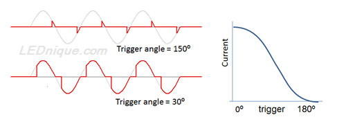
Figure 1 shows a typical triac dimmer for incandescent lamps. Initially the triac, T1, is off.
As the mains voltage rises C1 starts to charge up at a rate determined by the setting of R1; the lower the value of R1 the faster C1 charges up.
When the voltage on C1 reaches about 20 V the DIAC breaks down and the charge in C1 flows into the trigger of T1 turning it on.
One of the triac’s characteristics is that once triggered the triac will remain on until the current falls below the hold-on value which is close to zero (typically about 50 mA).
The result is a phase-angle controlled waveform as shown in Figure 2. If the triac is triggered late in the cycle (upper trace) the RMS voltage is low. If triggered early in the cycle (lower trace) the RMS voltage will be high. Note that the response is not linear.
Figure 2. The upper trace shows the trigger delayed close to the end of the cycle. The resultant effective voltage is low. The lower trace shows the trigger close to the start of the cycle. This will result in close to full voltage. The relationship between phase angle delay and resultant RMS voltage is graphed on the right.
Fluorescent lights
As fluorescent lights need a minimum voltage, and both compact fluorescents and LEDs use electronics which rectifies the peak voltage provided, the conventional phase-angle control dimmer fails to dim them.
Ballast fluorescent lights would dim as the voltage reduced a little but then probably flicker and fail to light at all as the tube temperature dropped at further reduced voltage. For high frequency flourescent, CCFL and LED, it all depends on how the control circuitry has been designed.
LED filament bulbs
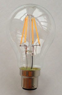
LED filament lamps look remarkably similar to tungsten filament lamps.
Generally these lamps should work well with dimmers as there are no onboard electronics. Read more about these in LED filament lamps.
Passive LED
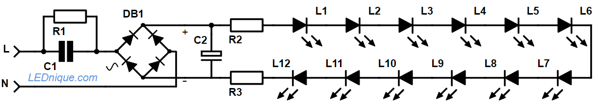
Some of the cheap LED mains lamps use a capacative voltage dropper to reduce the voltage and limit the current to the lamps. (A capacitor has a certain ‘impedance’ to AC – its AC resistance – given by \( Z = \frac {1}{2 \pi f C} \) where f is the mains frequency, 50 or 60 Hz and C is the capacitance in F.)
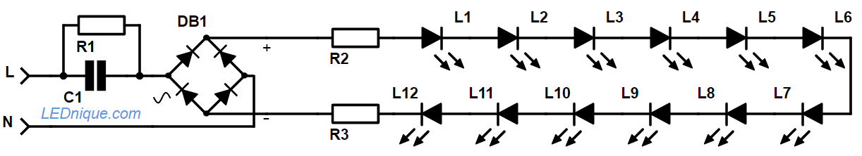
A typical arrangement for a cheap capacitive dropper power-supply LED bulb.
How it works:
C1 is chosen to limit the current to the rectifier.
R1 is a high value and has no function in the circuit other than to discharge C1 when the power is switched off.
Bridge rectifier, DB1, converts to DC.
R2 and 3, in conjunction with C1, set the current through the LEDs.
Note that since all are in series that the same small current powers them all.
These bulbs should respond well to a dimmer as there are no components storing charge during the mains cycle. The problem is that it is almost impossible to tell without a test.
If the manufacturer has included a smoothing capacitor a further complication arises.
Note that if a smooting capacitor such as C2 is included after the rectifier that the dimmer won’t appear to do anything until the control is adjusted below 50%. This is because the capacitor charges up fully at peak mains even if it hasn’t been on up to 90° into the half-cycle. (See Figure 1.) From 90° to 180° the peak voltage drops so the lamp will dim in proportion.
Constant power / current lamps
Lamps designed to work at full output over a wide range of input voltages will not behave well with dimmers. Typically these will use an internal switched mode power supply which will attempt to keep the LEDs running at designed current until the voltage goes below the minimum specified.
Since the power (\( P = VI \)) is constant across the range of supply voltages the current will increase as the voltage decreases. If the supply voltage drops below the minimum specification the power supply can no longer maintain the output current. At this point the LEDs may dim or flicker or just go out.
Smart dimmable bulbs
Note that some dimmable LED bulbs are available. They rectify the peak voltage, take their control input as the width of the pulse from the TRIAC dimmer, and program their current output accordingly. Some clever types even change their colour temperature according to the dimmer setting, cool white when full on, and warm white when dimmed.
For successful dimming you need to match the dimmer and lamp or power-supply.
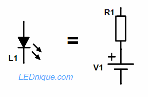
LEDs do not have a linear relationship between current and voltage so they cannot be modeled as simply as a resistor using Ohm’s Law, \( V = IR \). We can, however, make a simplification and model them over a range of currents as a combination of a resistor and a voltage source.
Figure 1. An LED can be approximated as a resistor with a fixed voltage source.
If we look at a typical LED IV curve we can see that it is approximately linear over much of its useful range. This allows us to model the LED as a resistor and voltage source.
Figure 2. LED equivalent circuit model.
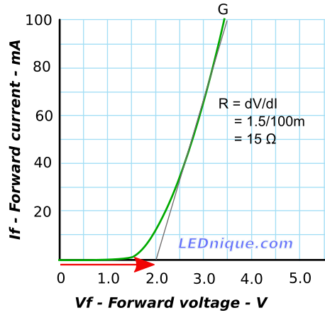
In Figure 1 the grey line is reasonably close to the LED curve from 20 mA to 100 mA. We can work out the resistance that this represents from Ohm’s law \( V = IR \) but in this case we will look at the change in voltage and current in the area of interes.
We can also see that the line crosses the X-axis at Vf = 2.0 V. Our equivalent circuit for this region of interest is (referring to Figure 2) R1 = 15 Ω and V1 = 2.0 V.
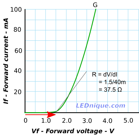
Figure 3. For the lower end of the IV curve we can create another approximation.
If we are interested in the lower current range of the LED, 1 to 20 mA, for example, we can calculate again. In this case the ends of the grey line have differences of 1.5 V and 40 mA giving a slope of 37.5 Ω. The voltage source becomes 1.5 V.
LEDs fall into to general methods of light generation – direct and indirect.
The direct LEDs emit light directly from the diode junction. These include most visible colour LEDs and the IR and UV types too.
The indirect LEDs have phosphors which convert the LED’s monochromatic light into a broad spectrum of light. These were commonly used in early white LEDs as blue was difficult or expensive to create.
Direct emission LEDs typically have a turn-on time in single-digit nanoseconds, longer for bigger LEDs. Turn-off times for these are in the tens of nanoseconds, a bit slower than turn-on. IR LEDs typically show the fastest transition times.
Special purpose LEDs are available, whose junction and bond-wire geometries are designed specifically to permit 800 picosecond to 2 nanosecond pulses. For even shorter pulses, special purpose laser diodes, in many ways operationally similar to LEDs, work all the way down to 50 picosecond pulses.
Phosphor type LEDs have turn-on and turn-off times in the tens to hundreds of nanoseconds, appreciably slower than direct emission LEDs. This is due to the time taken to excite the phosphors enough to emit light.
The dominant factors for rapid LED switching are not just the LED’s inherent emission transition times:
Inductance of the traces causes reduced rise and fall times. Longer traces = slower transitions.
Junction capacitance of the LED itself is a factor(#2). For instance, these 5mm through-hole LEDs have a junction capacitance of 50 pF nominal. Smaller junctions e.g. 0602 SMD LEDs have correspondingly lower junction capacitance, and are in any case more likely to be used for screen backlights.
Parasitic capacitance (traces and support circuitry) plays an important role in increasing the RC time constant and thus slowing transitions.
Typical LED driving topologies e.g. low-side MOSFET switching, do not actively pull the voltage across the LED down when turning off, hence turn-off times are typically slower than turn-on.
As a result of the inductive and capacitive factors above, the higher the forward voltage of the LED, the longer the rise and fall times, due to the power source having to drive current harder to overcome these factors. Thus IR LEDs, with typically the lowest forward voltages, transition fastest.
Thus, in practice the limiting time constants for an implemented design can be in the hundreds of nanoseconds. This is largely due to external factors i.e. the driving circuit. Contrast this with the LED junction’s much shorter transition times.
To get an indication of the dominance of the driving circuit design as opposed to the LEDs themselves, see this recent US government RFI (April 2013), seeking circuit designs that can guarantee LED switching time in the 20 nanosecond range.
Credits: Anindo Ghosh on electronics.stackexchange.com.
An LED can be used as a simple stepper motor continuity tester. Motors act as generators when driven and a typical stepper motor will generate a low voltage / low current output when spun by hand. This is enough to light an LED.
The technique can be used to figure out motor winding pairs and continuity.
Other methods of checking windings are:
Short one winding. (In the video example that would require replacing the LED with a link.) You should feel a very marked increase in resistance to rotation and feel “cogging” as each tooth of the rotor passes a pole. Repeat for the other winding.
Use a multimeter. This will be more useful than the video LED test in identifying the windings in, for example, centre-tapped uni-polar motors as each coil’s end to end resistance will be double that of centre to end resistance. It also allows comparison between windings.
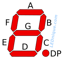
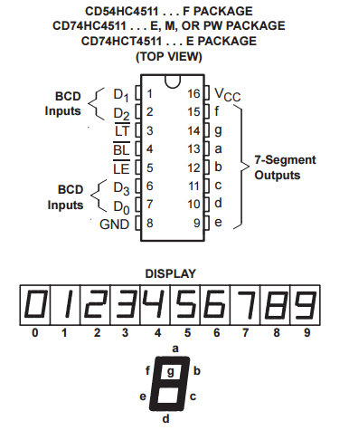
Figure 1. Standard 7-segment display layout and segment identification. The decimal, if supplied, point requires an eight LED.
7-segment (or “seven-segment) LED displays are commonly used to display digital information. Each segment consists of one or more LEDs and can be lit independently of all the others to form the digits 0 to 9. A limited range of alphabetic characters can also be formed but these are of mixed case and can be difficult to read.
The standard segment identification is shown in Figure 1 and segments are named A to G starting at the top and going clockwise with G being the centre segment.
Typically the displays have a common pin for all the LED anodes or cathodes. Eight pins will suffice for a true seven-segment display whereas nine are required for one with a decimal point.
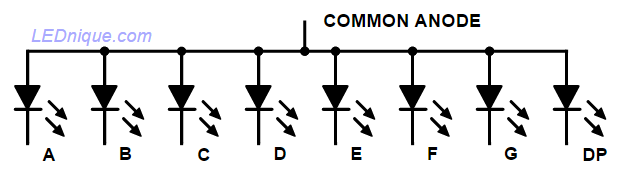
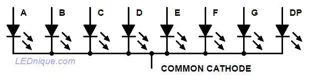
Figure 2. As might be expected, package pin-count is reduced by using a common pin for one side of all the LEDs. In this case a common anode is used.Figure 3. A common cathode display. These have the advantage that, for multiplexed displays, the digit can be strobed using an NPN transistor in the cathode connection to ground.
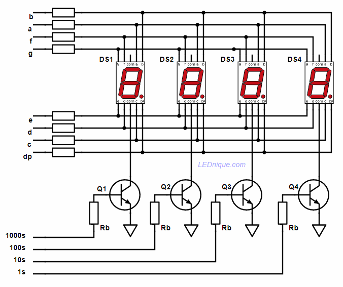
By multiplexing seven-segment displays the number of pins required to drive the displays can be reduced. In the scheme of Figure 4 the segments are driven high by the micro-controller. The required segments for digit 1 are set on lines A to G and Q1 strobed (turned on briefly). Then the required segments for digit 2 are turned on and Q2 is strobed, etc. The sequence is run quickly enough that all digits appear to be continuously lit due to persistance of vision.
When multiplexing displays in this manner it is normal to run at a current higher than nominal. This is acceptable because the segments will be powered for a maximum of 25% of the time – 25% duty-cycle.
Note that 32 segments can be controlled using only 12 outputs from the controller. This efficiency in hardware and PCB layout is what makes multiplexing so popular.
Reducing controller pins
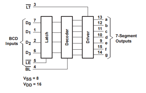
Figure 5. The 4511 BCD to 7-segment latch / decoder / driver.
By using a latch / decoder / driver such as the 4511 decoder (datasheet) the designer has many more options for display. By using the BCD decoder only four lines are required to drive the seven segments.
Figure 6. 4511 function diagram.
BL: blanking. Pull low to turn all segments off. Display: blank.
LT: lamp-test. Pull low to turn all segments on. Display: ‘8’.
LE: latch enable. Pull low to read the inputs and pass through to the seven segment outputs. Pull high to latch the outputs.
Note that BCD values above ‘9’ are considered void and the display will be blank. This renders the 4511 unsuitable for hexadecimal display.
The 4511 can source or sink current for the displays. See the datasheet for ratings.
Flicker-free 7-segment display
Figure 6. By using a 4511 latch per display a flicker-free display is possible.
Figure 5 shows how to use a 4511 latch per digit. In this case the data for each digit is set up in turn on D0 to D3 and the digit’s /LE (latch enable) pin is pulled low. The seven-segment display will immediately update and will be latched when the /LE pin is pulled high again. This, for example, would allow the micro to handle other tasks without having to update the display until required. The D0 to D3 IO pins could even be used as inputs with suitable input resistors while the diplay update is not required.
Note that the display decimal points are not controlled by the 4511. This leaves the designer with several options:
No decimal point.
A fixed decimal point by wiring one of the DP pins to Vss.
Program controlled decimal point. This will require one extra controller output pin per decimal point.
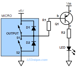
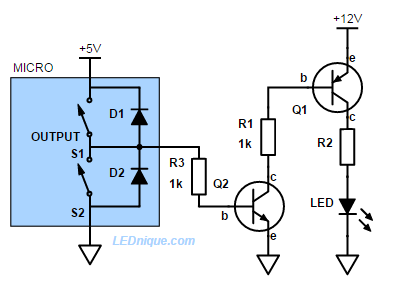
Figure 1. On the face of it, this looks like a reasonable means of achieving a high-side switch. But watch those diodes!
The NPN common emitter configuration makes it easy to make a low-side to switch loads connecte to positive supply. It seems logical to assume that a PNP transistor could provide a mirrored circuit to make a simple high-side switch. The circuit of Figure 1 will work fine provided that \( V_{SS} \leq V_{MICRO} \) (or whatever voltage the micro is running on).
Figure 2. The protection diodes on most logic chips creates a sneak-path to positive supply. This will keep the PNP transistor permanently turned on and may damage the chip.
If If \( V_{SS} > V_{MICRO} \) then the output protection diodes built into the chip provide a sneak path for the base current. The e-b junction of Q1 will be forward biased and current will flow through it, R1 and D1 to the micro supply. Q1 will turn on and LED will light and will not switch off.
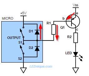
We can fix this at the expense of adding an NPN low-side switch.
Figure 3. To drive a high-side transistor from a GPIO pin we need a level translator. An NPN transistor does the job nicely.
In Figure 3 the micro drives Q2 as in a normal NPN low-side switch. When Q2 is turned on current will flow from the base of Q1, through R1 and Q2 to ground. Q1 will turn on and the LED will light.
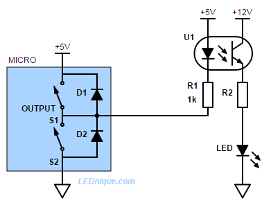
Figure 4. An opto-isolated high-side driver.
In Figure 4 the problem has been solved by using an opto-isolator. Now there is no chance of the 12 V supply back-feeding into the micro.
Note that in this example the grounds are common between the two circuits. They could, however, be separated for complete isolation. See “A basic application” on Opto-isolators – intro for an example.
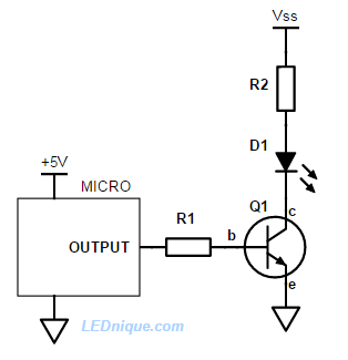
For various reasons it is often necessary to control LEDs supplied by a voltage higher than the micro-controller can supply or withstand. In these cases the most common solution is to use an NPN transistor as a switch or driver to buffer between the two parts of the circuit – the low-voltage control circuit and the high-voltage load circuit.
An NPN transistor can be used to act as a switch controlled by a low-voltage micro-controller switching a high voltage or high-current load.
When there is no current flowing into the base (b) of Q1 the transistor is off and no current flows from the collector (c) to the emitter (e). As we increase the current into the base of the transistor the transistor starts to turn on and its resistance falls allowing current to flow from Vss, through R2, D1 and Q1 to ground.
Small signal transistors have a “current gain” of 50 to 300. This means that for 0.1 mA into the base we should be able to get 5 to 30 mA to flow through the collector. The relationship is given by the equation \( I_C = h_{FE}I_B \) where \( I_C \) is the collector current, \( h_{FE} \) is the current gain and \( I_B \) the base current.
At first glance it seems that we could control the LED current to any value we wanted by controlling the base current. Unfortunately there is enough variation between transistors and the fact that this parameter is temperature dependent that this would not be a good reliable and repeatable design. (It might be OK for a one-off project provided you were confident you would never have to replace the transistor.)
Instead we inject more than enough current into the base to turn the transistor “hard” into saturation: the collector voltage drops as low as it can go – typically below 0.2 V.
Example 1 (NPN driver)
Our micro-controller output is a 5 V signal.
Vss is 12 V.
The LED, D1 requires 100 mA and will have a forward voltage of 2.8 V at that current.
Q1 has a \( h_{FE} \) of somewhere around 100.
R1
We want to ensure that the transistor saturates to give minimum voltage drop between the collector and emitter. In saturation we’ll assume that a current gain of 10 to 20 is likely. To guarantee saturation we should design for a base current of 5 to 10 mA. This will be fine for most micro-controllers (but always check the specification). The base voltage will rise to about 0.6 V when forward biased so the voltage across R1 will be 5 – 0.6 = 4.4 V. We can calculate (from Ohm’s Law) \( R_1 = \frac {V}{I} = \frac {4.4}{0.005} = 880\,\Omega \) and it would be half of that at 10 mA. We can go somewhere in-between with a 560 Ω or 680 Ω resistor.
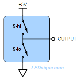
Figure 1. Simplified logic output stage showing the high-side and low-side switches.
Most micro-controllers and logic families have output stages which can connect the output to the positive supply or to ground. This allows the micro to put a definite ‘high’ (+5 V in this example) onto the output or a definite ‘low’ (ground) rather than let it float which could cause problems if the output is feeding into another device. Naturally, only one of the switches should be closed at any time. In this article we look at high-side versus low-side switching.
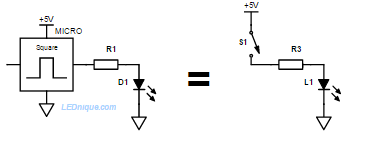
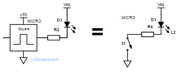
Figure 2. To power an LED connected to ground the micro simply connects the output to positive supply. In this configuration we use the upper transistor in the output stage to supply current to the output – much in the same way as S1 in the equivalent circuit.
Most micros can now source 10 to 20 mA safely on their GPIO1 pins. This is ample current to light an LED brightly. All that is require is to decide whether to source current for the LED or sink current.
Figure 3. To power an LED connected to positive supply the micro simply connects the output to ground. In this configuration we use the lower transistor in the output stage to sink current from the LED to ground – much in the same way as S1 in the equivalent circuit.
Some more detail
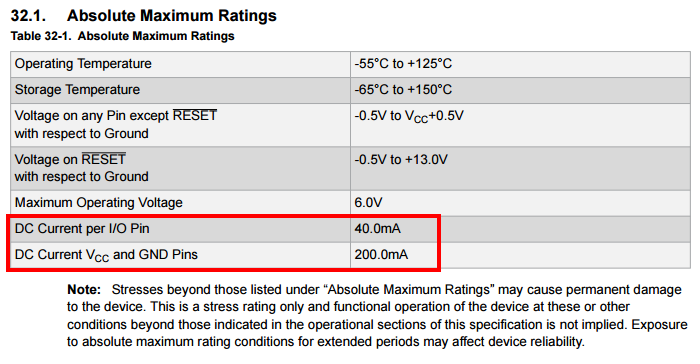
The switches in real devices will be constructed with transistors. These are imperfect and have various limits that we have to be aware of, such as maximum current and source resistance. For example, the ATmega328P used in the Arduino Uno states that the IO pins can handle up to 40 mA subject to a maximum total of 200 mA for the whole chip.
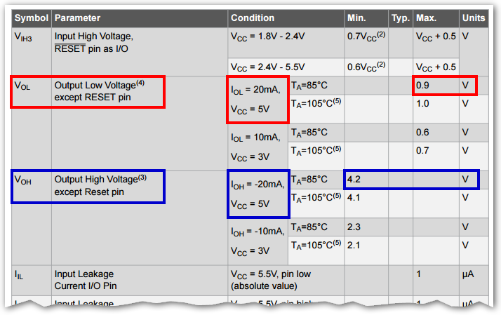
Figure 4. The absolute maximum current handling capability of the ATmega328 and 328P micro.Figure 5. At 20 mA the ATmega328P output is pulled up to 0.9 V above zero when low and about 0.8 V below positive supply when high.
Note on Figure 5 the \(V_{OL}\) voltage – the actual voltage measurable on the output pin (red) – when switched low and sinking 20 mA that the voltage won’t be zero as might be expected but could be as much as 0.9 V above ground. This is due to the voltage drop across the low-side transistor switch in the output.
Similarly, when the output is switched high and sourcing 20 mA the output won’t be +5 V (the test condition power supply voltage) but could be as much as 0.8 V below that.
It’s worth being aware of this as it could be significant in some low-voltage applications where there isn’t much “headroom” between the voltage required by the LED and that of the power supply.
Example 1 – 5 V supply
Figure 3. Using the LED IV curves to find the required R value for a green LED at 20 mA.
Figure 6 shows that the LED at 20 mA will have a forward voltage drop of about 2.2 V. If the supply voltage is 5 V then the resistor has to drop \(5 – 2.2 = 2.8\,\mathrm V \). The required value is \( R = \frac {V}{I} = \frac {2.8}{0.02} = 140\,\Omega \). The nearest standard value of 150 Ω will do fine.
The resistance calculation will be the same for the current sinking option of Figure 2.
Example 2 – 3.3 V supply
When running from a 3.3 V supply the headroom becomes substantially limited.
As the supply voltage is decreased to 3.3 V the “headroom” for driving an LED is reduced and, when output droop is taken into consideration, the device may not be able to provide enough current.
Here we can see that the LED is still requiring 2.2 V leaving 3.3 – 2.2 = 1.1 V for the resistor. If this 3.3 V chip’s output were to droop by, say, 0.5 V then that leaves us with only 0.6 V for the resistor: \( R = \frac {V}{I} = \frac {0.6}{0.02} = 30\,\Omega \).
The problem with this is that a low-value resistor is not a very good constant current source. If the forward voltage, \( V_F \) of the LED decreased by 0.1 V due to temperature or batch to batch variation then the voltage would go to 0.7 V and I would increase from 20 mA to \( I = \frac {V}{R} = \frac {0.7}{30} = 23\,\mathrm mA \). This might push the device a little closer to the absolute maximum ratings.
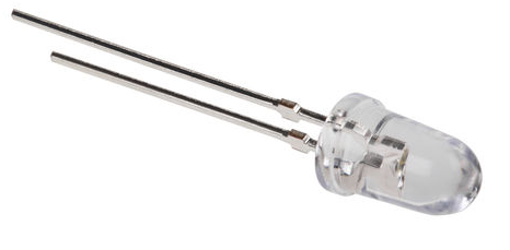
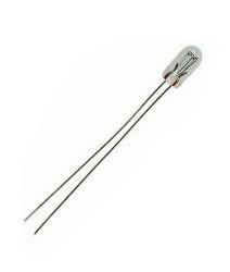
Varying the lead length on the LED packages eases identification of the pins. It also serves to ease insertion into PCBs. The longest lead is located in the board first, followed by the next longest lead, etc., gradually advancing the component into the board until all are located and the LED pushed in to the required depth.
A 3-pin LED with three different lead lengths. The datasheet will specify the LED colours associated with each lead.
Note that many of the packages have shoulders on the leads to provide a positive stop against the PCB for ease of alignment, etc.
T-sizes
Figure 3. A T1.75 or T1-3/4 incandescent bulb. The diameter is 1/8″ x 1.75.
Early LEDs were made to conform to standard “T” sizes. The “T” designation indicated tubular shape and the numbers after indicated the tubular diameter in 1/8″ multiples. The original LEDs were made in T1-3/4 or T1.75 (5.5 mm – 5 mm nominal) and later in T1 (1/8″ = 3 mm) packages.