Opto-triacs or solid-state relays (SSR) consist of an infra-red LED and a triac in one package. The LED is switched on and off by a low-power DC control circuit and this switches the triac which can be used to control AC devices up to mains voltages.
Opto-triacs provide electrical isolation between the control circuit and the AC circuit.
Opto-triacs are available in “random” and zero-cross types.
Since the LED portion of the opto-triac is an infra-red LED the series resistor value can be calculated if the required current is known. (Get this value from the device datasheet.)
Safety
Triacs are usually used on mains voltage. This presents a serious risk of electrocution. Working on mains voltage is not recommended for beginners in electronics.
How triacs work
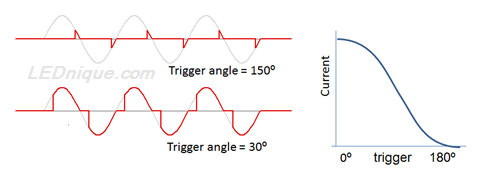
Triacs are semi-conductor switches that can be turned on by a pulse on the gate or trigger pin. Once turned on they stay on until the current drops below the hold-on value. By delaying the turn-on point until some time after the voltage crosses zero volts – the zero-cross point – the voltage can be adjusted although it is no longer sinusoidal.
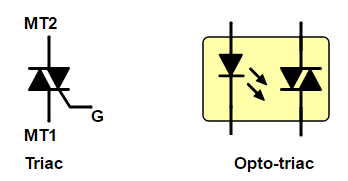
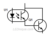
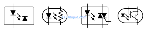
Figure 1. The upper trace shows the trigger delayed close to the end of the cycle. The resultant effective voltage is low. The lower trace shows the trigger close to the start of the cycle. This will result in close to full voltage. The relationship between phase angle delay and resultant RMS voltage is graphed on the right.Figure 2. Schematic symbols for a discrete triac and an opto-triac. Note that since the opto triac is optically triggered it (usually) does not have a gate or trigger pin.
The devices shown in Figure 2 can be used to give variable phase-angle control as shown in Figure 1. (These are sometimes called “random” opto-triacs or SSRs but “random” is a misnomer as usually the trigger point is anything but random and is controlled. What is meant is “variable” trigger-point.)
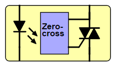
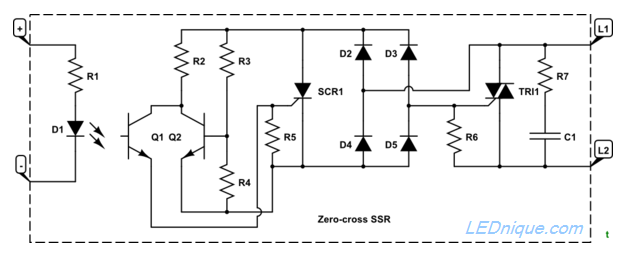
Figure 4. A zero-cross opto-triac or SSR.
When the LED of the zero-cross opto-triac it turned on the zero-cross detection circuit will wait until the voltage is very close to zero before switching on the triac. This minimises switching noise and electro-magnetic interference (EMI) to neighbouring equipment.
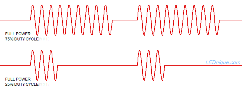
Figure 4. With zero-cross switching the result is that the waveform consists of multiple complete half-cycles.
How zero-cross detection works
Figure 5. Internals of a zero-cross detection circuit based on the G3MB-202P with 5V input.
If \(V_{L1−L2}\) is low (above but close to zero) and Q1 is turned on by photo-action from D1 then SCR1 will be triggered. This in turn will pass enough current through R6 to bring TRI1 gate voltage high enough to trigger.
When voltage exceeds a certain level Q2 will be biased on. The collector voltage will fall and there won’t be enough to turn on SCR1 even if Q1 subsequently turns on.
The effect is that TRI1 can’t turn on unless it is triggered close to the zero cross.
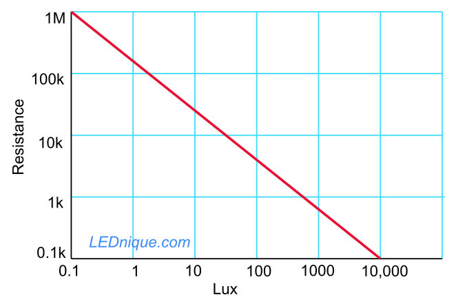
Resistance decreases with increasing light levels.
Typically > 1 MΩ when dark and < 1 kΩ in high light levels.
Response time of 2 – 50 ms. (Much slower than photo-transistors.)
They have a “light history”. Characteristics change a little as they acclimatise after long periods in darkness.
LDRs are more sensitive to certain wavelengths (colours). The CdS types are most sensitive to green.
Details
LDRs, light depenedent resistors or photo-resistors are often used with LED circuits as simple photo-detectors.
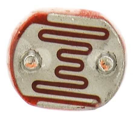
Figure 1. A Silonex NSL-19M51 LDR top view. Note that the brown zig-zag stripe forms a “border crossing” between the two terminals. The number of charge carriers that make it across the border is proportional to the amount of light hitting the border zone.
In dark conditions the resistance between the terminals is high – up to 1 MΩ or so. The resistance falls with increasing light levels down to a few hundred ohms at high brightness.
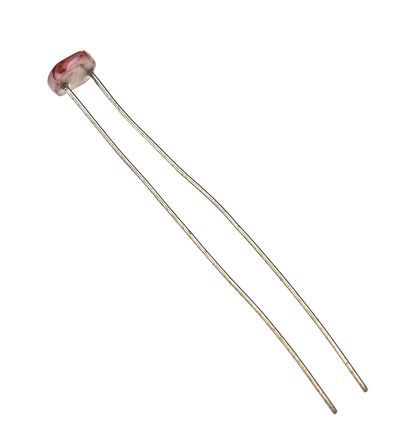
Figure 2. Typical LDR packaging.Figure 3. Graph of resistance versus light level.
Lighting condition
From (lux)
To (lux)
Mean value (lux)
Pitch Black
0
10
5
Very Dark
11
50
30
Dark Indoors
51
200
125
Dim Indoors
201
400
300
Normal Indoors
401
1000
700
Bright Indoors
1001
5000
3000
Dim Outdoors
5001
10,000
7500
Cloudy Outdoors
10,001
30,000
20,000
Direct Sunlight
30,001
100,000
65,000
Spectral response
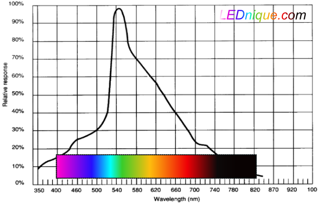
LDR Sunram CdS spectral response with visible light spectrum superimposed.
The common CdS (cadmium sulfide) LDRs have peak spectral response at about 550 nm which is the green region of the visible spectrum. Note that if illuminating the LDR with an LED that a red LED might give only about 30% of the response of a green LED on the same current.
Understanding the datasheet
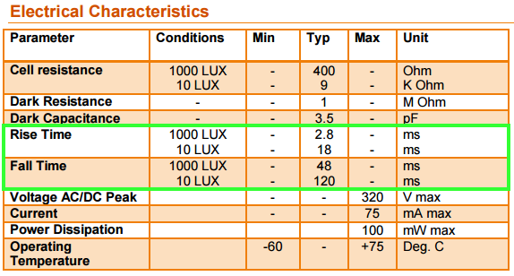
The Luna datasheet for the NSL-19M51 gives the following figures.
LDR NSL-19M51 opto electrical specifications.
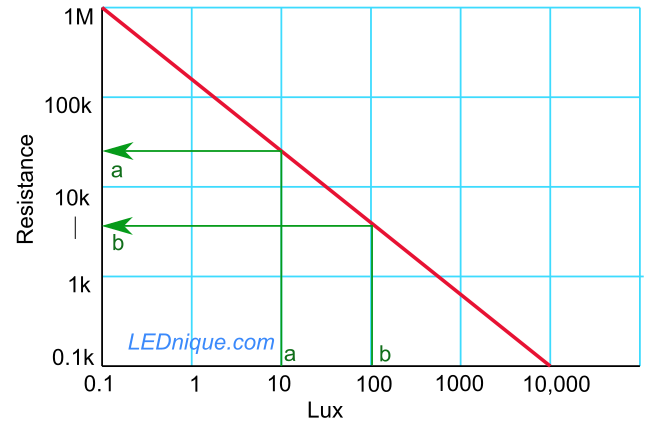
Note the wide variation in resistance at 10 lux – 20 to 100 kΩ.
Note a “typical” resistance at 100 lux of 5 kΩ.
Note that maximum dark resistance is specified for 10 s after removal of light. This suggests that the device response is slow.
The gamma characteristic is a measure of the slope of the resistance versus lux relationship. (See below.)
LDR gamma characteristic
LDR gamma graphical calculation.
LDR gamma characteristic is a measure of the rate of change of resistance over range of light variation. Typically the gamma is specified for the range 10 to 100 lux and calculated as
Gamma values of 0.6 to 0.8 are common for CdS LDRs. A gamma tolerance of ±0.1 is common.
For the digital ON-OFF applications such as flame detectors, LDRs with steep slopes to their resistance versus light intensity curves are appropriate. For analog or measurement types of applications such as exposure controls for cameras, LDRs with shallow slopes may be better suited.
Response times
LDR rise and fall times.
The slow response times of LDRs makes them unsuitable for data transmission, for example, but can be an advantage in other circuits such as flame detectors or audio effects where the slow response smoothes out the signal being monitored or controlled.
Light history
A photocell which has been stored for a long time in the light will have a considerably higher light resistance than if it was stored for a long time in the dark. Also, if a cell is stored for a long period of time at a light level higher than the test level, it will have a higher light resistance than if it was stored at a light level closer to the test light level. This effect can be minimized significantly by keeping the photocell exposed to some constant low level of illumination (as opposed to having it sit in the dark). This is the reason resistance specifications are characterized after 16 hours light adept. (Source.)
You can fabricate an opto-isolator using components from the scrap bin. This may be useful in special circumstances or when you need an opto-isolator in a hurry but don’t have one to hand.
All transistors exhibit the photo-transistor effect and are packaged in opaque material to prevent stray light interfering with their operation in circuit. It is possible to remove the top from the metal can packages to expose the transistor chip. By closely coupling an LED as shown in Figure 1 it is possible to improvise an opto-isolator. The current transfer ratio (the ratio of the transistor current to that of the LED) might not be too good but it may be adequate in certain applications or with modification.
Figure 1. LED glued to opened metal-can BC108 NPN transistor.Figure 2. The DIY opto-isolator should be wrapped with opaque heatshrink to prevent ingress of stray light.
Increasing the opto-isolator current transfer
Figure 3. Increasing the current transfer using a Darlington transistor.
By adding a second transistor to form a Darlington pair the current transfer ratio can be improved – by approximately the current gain of the second transistor.
Be aware of two problems with this approach:
The collector-emitter voltage drop will be at least 2 × 0.7 V as there are now two base-emitter junctions in the Q1 bias path.
The high-frequency response will be affected as there is a second delay in the circuit.
An opto-isolator is a component that transfers electrical signals between two isolated circuits by using light. This allows transmission of electrical signals between systems of different voltages with complete electrical isolation up to the rated isolation voltage. A 5 V logic signal, for example, might switch a mains circuit using an opto-isolator without risk of the mains feeding into to the low-voltage logic. 1 kV isolation is common for mains powered circuits.
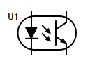
Figure 1. Opto-isolator schematic symbol showing the LED and photo-transistor elements.
The most common type of opto-isolator consists of an LED and a photo-transistor combined in an opaque package. In operation the photons from the illuminated LED that hit the base-collector junction in the transistor generate electrons and these are injected into the base, turning on the transistor.
Usually opto-isolators transfer digital (on-off) signals, but some techniques allow them to be used with analog signals.
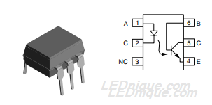
Figure 2. DIL opto-isolator package and pinout.
Figure 2 shows a typical pinout for a 6-pin DIL single opto-isolator package. This one makes the transistor’s base available on pin 6 but this is not always the case – particularly on high-density packages.
A basic application
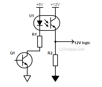
Figure 3. Switching a 12 V circuit with a 5 V control signal.
Figure 3 shows a simple application where a 5 V logic signal in one circuit is controlling a 12 V signal in another. When Q1 is switched on U1 LED will illuminate and the collector-emitter resistance will fall to a low value. The 12 V logic level will then switch from low to high.
Note the different ground symbols on the 5 V and 12 V circuits indicating isolated grounds.
Reading the datasheet
The information below is published in the Vishay 4N25 datasheet. As always, in most applications certain parameters become more significant than others. Careful reading of the datasheets and experience will be your guide.
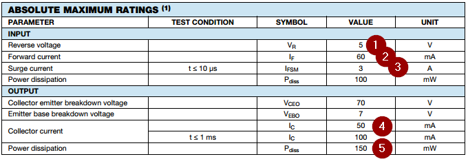
Absolute maximum ratings
Table 1. Essential reading.
From the Absolute Maximum Ratings section we can see:
(1) The maximum reverse voltage the LED can take is 5 V.
(2) The maximum continuous forward current is 60 mA.
(3) Surprisingly, perhaps, the LED peak current is 3 A but note well that this is for ≤ 10 µs. There will be a recovery time associated with this.
(4) The transistor output is capable of 100 mA continuous.
(5) Watch the output transistor power dissipation: if the transistor is not turned hard-on there will be a voltage drop across it and the power dissipation may rise. e.g., If there is 3 V across the output transistor then the maximum output current will be given by \(I_{max} = \frac {P_{max}}{V_{ce}} = \frac {150m}{3} = 50 \, \mathrm mA\).
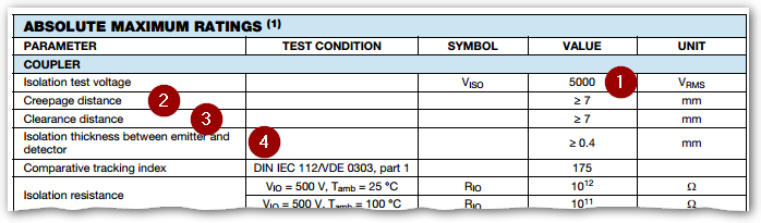
Isolation, creepage and clearance
Table 2. Isolation, creepage and clearance.
(1) 5,000 V isolation between the input and output.
(2) The creepage distance is 7 mm. This is the shortest distance along the surface of the package between any input and output pin.
Figure 4. Cross-section of an opto isolator. Creepage distance is measured along the outside of the package while clearance is the shortest distance through the air.
See Vishay’s Design Guidelines for Optocoupler Safety Agency Compliance for details on this.
(3) The clearance distance is the shortest distance through the air between the any input and output. Note that in most cases the PCB pad radius will reduce this distance significantly.
(4) The internal insulation thickness.
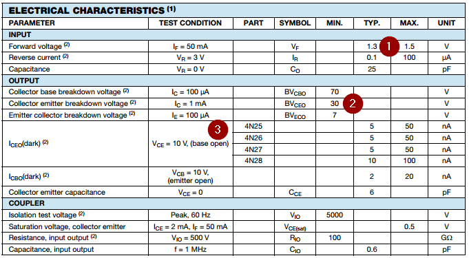
Input and output specifications
Table 3. Electrical characteristics.
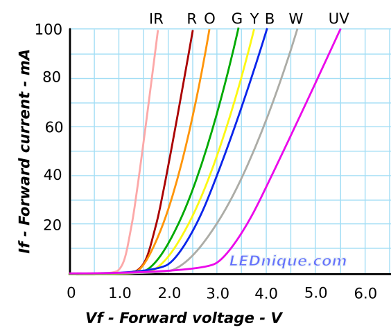
(1) The forward voltage of the LED is only 1.3 V. From this we can infer that it is an infra-red type – see Figure 5 – but this is stated in the description on page 1.
(2) The maximum voltage we can switch with this device is 30 V.
(3) At 10 V there will be up to 50 nA leakage current between the collector and emitter when the LED is dark (unpowered).
Other parameters such as capacitance may be important at high frequencies.
Figure 5. Typical IV curves for various colours of LEDs. From this we can see that only the IR LED could result in the 1.3 to 1.5 V forward voltage at 50 mA. The forward voltage of an LED is temperature dependent and will decrease with increasing temperature.
Current transfer ratio
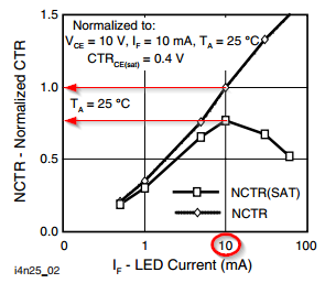
Table 4. DC current transfer ratios.Figure 6. Current transfer ration (CTR) as a function of LED current. Note datasheet has CTR curves for other temperatures also.
Table 4 and Figure 6 show us that for this device when the LED is run at 10 mA we can expect to get only 2 to 5 mA maximum out of the transistor. If more current is required then further amplification is required – e.g., the Darlington arrangement shown at the top of this page.
In most applications we design the circuit to drive the output transistor into saturation.
Switching characteristics
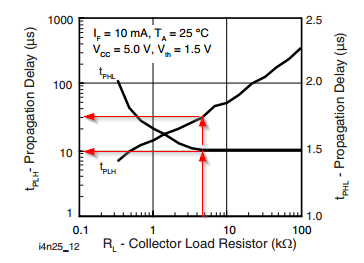
Table 5. The switching characteristics lead one to believe that a fixed delay of 2 µs is given.
While Table 5 gives the impression that a fixed time delay of 2 µs is given, Figures 7 and 8 show that the situation is more complex.
Figure 7. Propagation delay is different for high to low (PHL) and low to high (PLH). (Test configuration is a low side switch. See the datasheet Fig. 14.)
Figure 7 demonstrates that for a 4.7 kΩ load on a 5 V supply we could expect a 10 µs fall time (PHL) (photo-transistor turning on) but a 30 µs rise time (PLH) (photo-transistor turning off). This difference may be enough to cause problems in high frequency circuits or where accurate timing is required.
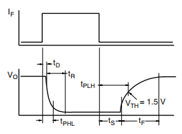
Figure 8. Timing diagram.
Other types of opto-isolator
Opto-isolators can be made using LED-photodiode, LED-LASCR, and lamp-photoresistor pairs.
Figure 9. Opto-isolator variants include (a) photo-diodes, (b) photo-resistors, (c) opto-triacs and (d) darlington opto-isolators.
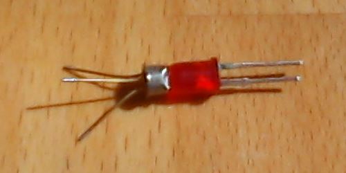
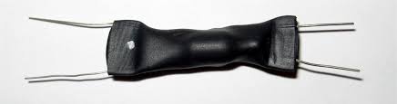
Opto-couplers were used before LEDs were invented. Fender guitar amplifiers, for example, used an old-fashioned neon lamp and light-dependent resistor (LDR) combination in the tremelo circuit of some models.
Figure 9. A neon and LDR opto-coupler. Note the outline of the neon lamp visible in the heatshrink tubing.
Alternate terminology
See also: optocoupler, photocoupler, or optical isolator.
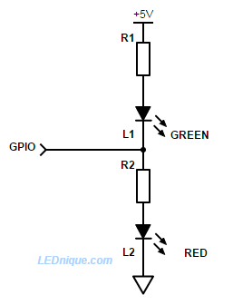
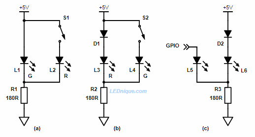
When the output is switched low current will flow from the positive supply via R1 and the L1, green, to the output pin. L1 will illuminate. L2, red, will be shorted out and will be dark.
When the output is switched high current will flow from the pin through R2 and L2. The red LED will illuminate and the green will be dark.
If the output is tri-stated (wired as an input or disconnected by program control) a current will flow through R1, L1, R2, L2 and both LEDs will glow dimly. On a 3.3 V device the voltage wouldn’t be high enough to illuminate both LEDs significantly so they would appear dark.
By rapidly (> 25 Hz should be enough) alternately switching the output high and low while varying the duty-cycle the red and green can be blended to give any colour in between the two.
Figure 2. A SunLED green-red integrated LED package with independent pinouts. See datasheet.Figure 3. RGB LEDs are available in 6-pin versions without common cathodes or anodes. e.g., Kingbright LED LF79WAEMBGMBW, 8 mm, RGB, 20–30 mcd.
Note that to incorporate the 6-pin LED of Figure 3 into the circuit of Figure 1 you would control two of the three LEDs but leave the third unconnected, driven permanently or from another GPIO.
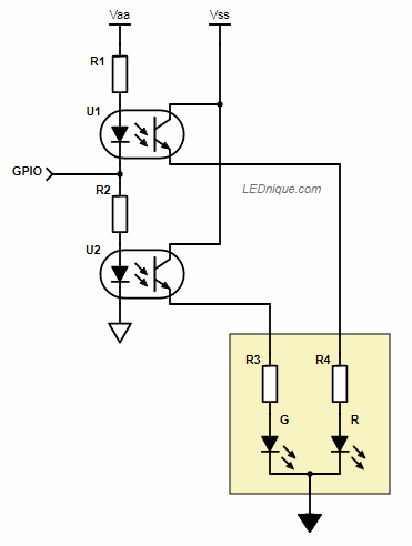
Figure 4. 1 GPIO – 2 opto-isolators.
The same trick can be used to switch isolated or non-isolated loads using opto-isolators. When the GPIO is high U2 will be turned on. When low, U1 will be turned on.
1 switch, 2 LEDs
Figure 5. 1 switch or GPIO and 2 LEDs.
In (a) above the green LED is normally lit. There will be about 2.1 V across the LED.
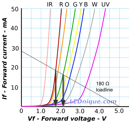
When S1 is closed the red LED will turn on but since it’s forward voltage drop is only about 1.75 V the current in the green will drop very low. A look at the load-line graph shows us why.
Figure 6. Load-line for red and green LEDs in parallel shows that the red drops the voltage enough that little current passes through the green LED.
When the red LED is in circuit the LED voltage drops to 1.75 V or so. At this voltage the green only passes a couple of mA and will be off or dim.
If you want the circuit to operate the other way around as in Figure 5b then you need to induce further voltage drop. D1 achieves this. Now the combination of D1 and L3 will drop about 0.7 + 1.75 = 2.45 V. When the green is switched on there won’t be enough forward voltage to light the red (brightly).
The diode can be added to Figure 1a to reduce current further if the reduced current proves to be too bright.
The circuit will work with a GPIO output as shown in Figure 5c. In this case the additional diode, D2, will almost certainly be required as the GPIO will not reach +5 V when under load.