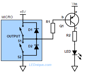
Figure 1. On the face of it, this looks like a reasonable means of achieving a high-side switch. But watch those diodes!
The NPN common emitter configuration makes it easy to make a low-side to switch loads connecte to positive supply. It seems logical to assume that a PNP transistor could provide a mirrored circuit to make a simple high-side switch. The circuit of Figure 1 will work fine provided that \( V_{SS} \leq V_{MICRO} \) (or whatever voltage the micro is running on).
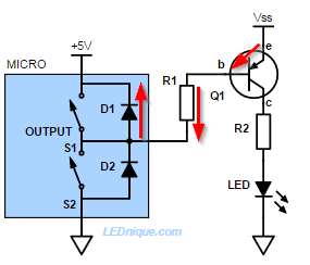
Figure 2. The protection diodes on most logic chips creates a sneak-path to positive supply. This will keep the PNP transistor permanently turned on and may damage the chip.
If If \( V_{SS} > V_{MICRO} \) then the output protection diodes built into the chip provide a sneak path for the base current. The e-b junction of Q1 will be forward biased and current will flow through it, R1 and D1 to the micro supply. Q1 will turn on and LED will light and will not switch off.
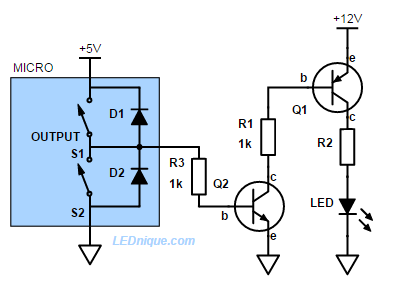
We can fix this at the expense of adding an NPN low-side switch.
Figure 3. To drive a high-side transistor from a GPIO pin we need a level translator. An NPN transistor does the job nicely.
In Figure 3 the micro drives Q2 as in a normal NPN low-side switch. When Q2 is turned on current will flow from the base of Q1, through R1 and Q2 to ground. Q1 will turn on and the LED will light.
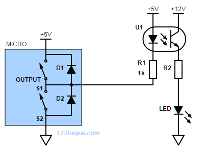
Figure 4. An opto-isolated high-side driver.
In Figure 4 the problem has been solved by using an opto-isolator. Now there is no chance of the 12 V supply back-feeding into the micro.
Note that in this example the grounds are common between the two circuits. They could, however, be separated for complete isolation. See “A basic application” on Opto-isolators – intro for an example.
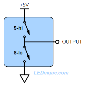
Figure 1. Simplified logic output stage showing the high-side and low-side switches.
Most micro-controllers and logic families have output stages which can connect the output to the positive supply or to ground. This allows the micro to put a definite ‘high’ (+5 V in this example) onto the output or a definite ‘low’ (ground) rather than let it float which could cause problems if the output is feeding into another device. Naturally, only one of the switches should be closed at any time. In this article we look at high-side versus low-side switching.
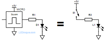
Figure 2. To power an LED connected to ground the micro simply connects the output to positive supply. In this configuration we use the upper transistor in the output stage to supply current to the output – much in the same way as S1 in the equivalent circuit.
Most micros can now source 10 to 20 mA safely on their GPIO1 pins. This is ample current to light an LED brightly. All that is require is to decide whether to source current for the LED or sink current.
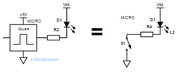
Figure 3. To power an LED connected to positive supply the micro simply connects the output to ground. In this configuration we use the lower transistor in the output stage to sink current from the LED to ground – much in the same way as S1 in the equivalent circuit.
Some more detail
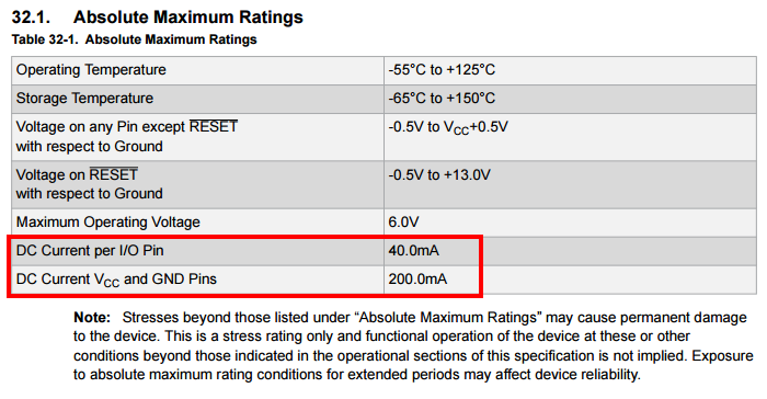
The switches in real devices will be constructed with transistors. These are imperfect and have various limits that we have to be aware of, such as maximum current and source resistance. For example, the ATmega328P used in the Arduino Uno states that the IO pins can handle up to 40 mA subject to a maximum total of 200 mA for the whole chip.
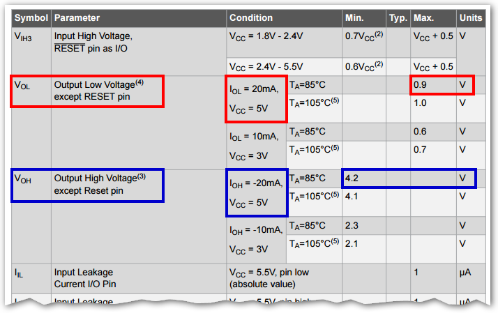
Figure 4. The absolute maximum current handling capability of the ATmega328 and 328P micro.Figure 5. At 20 mA the ATmega328P output is pulled up to 0.9 V above zero when low and about 0.8 V below positive supply when high.
Note on Figure 5 the \(V_{OL}\) voltage – the actual voltage measurable on the output pin (red) – when switched low and sinking 20 mA that the voltage won’t be zero as might be expected but could be as much as 0.9 V above ground. This is due to the voltage drop across the low-side transistor switch in the output.
Similarly, when the output is switched high and sourcing 20 mA the output won’t be +5 V (the test condition power supply voltage) but could be as much as 0.8 V below that.
It’s worth being aware of this as it could be significant in some low-voltage applications where there isn’t much “headroom” between the voltage required by the LED and that of the power supply.
Example 1 – 5 V supply
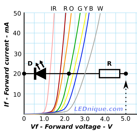
Figure 3. Using the LED IV curves to find the required R value for a green LED at 20 mA.
Figure 6 shows that the LED at 20 mA will have a forward voltage drop of about 2.2 V. If the supply voltage is 5 V then the resistor has to drop \(5 – 2.2 = 2.8\,\mathrm V \). The required value is \( R = \frac {V}{I} = \frac {2.8}{0.02} = 140\,\Omega \). The nearest standard value of 150 Ω will do fine.
The resistance calculation will be the same for the current sinking option of Figure 2.
Example 2 – 3.3 V supply
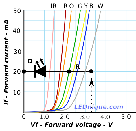
When running from a 3.3 V supply the headroom becomes substantially limited.
As the supply voltage is decreased to 3.3 V the “headroom” for driving an LED is reduced and, when output droop is taken into consideration, the device may not be able to provide enough current.
Here we can see that the LED is still requiring 2.2 V leaving 3.3 – 2.2 = 1.1 V for the resistor. If this 3.3 V chip’s output were to droop by, say, 0.5 V then that leaves us with only 0.6 V for the resistor: \( R = \frac {V}{I} = \frac {0.6}{0.02} = 30\,\Omega \).
The problem with this is that a low-value resistor is not a very good constant current source. If the forward voltage, \( V_F \) of the LED decreased by 0.1 V due to temperature or batch to batch variation then the voltage would go to 0.7 V and I would increase from 20 mA to \( I = \frac {V}{R} = \frac {0.7}{30} = 23\,\mathrm mA \). This might push the device a little closer to the absolute maximum ratings.