Figure 1. Standard 7-segment display layout and segment identification. The decimal, if supplied, point requires an eight LED.
7-segment (or “seven-segment) LED displays are commonly used to display digital information. Each segment consists of one or more LEDs and can be lit independently of all the others to form the digits 0 to 9. A limited range of alphabetic characters can also be formed but these are of mixed case and can be difficult to read.
The standard segment identification is shown in Figure 1 and segments are named A to G starting at the top and going clockwise with G being the centre segment.
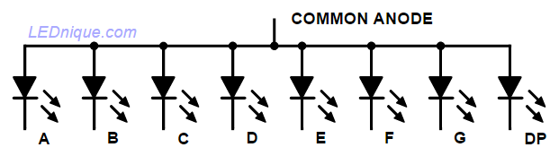
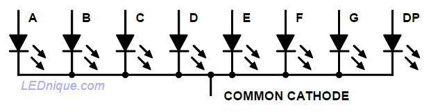
Typically the displays have a common pin for all the LED anodes or cathodes. Eight pins will suffice for a true seven-segment display whereas nine are required for one with a decimal point.
Figure 2. As might be expected, package pin-count is reduced by using a common pin for one side of all the LEDs. In this case a common anode is used.Figure 3. A common cathode display. These have the advantage that, for multiplexed displays, the digit can be strobed using an NPN transistor in the cathode connection to ground.
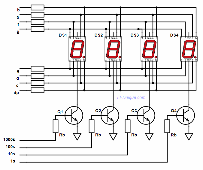
By multiplexing seven-segment displays the number of pins required to drive the displays can be reduced. In the scheme of Figure 4 the segments are driven high by the micro-controller. The required segments for digit 1 are set on lines A to G and Q1 strobed (turned on briefly). Then the required segments for digit 2 are turned on and Q2 is strobed, etc. The sequence is run quickly enough that all digits appear to be continuously lit due to persistance of vision.
When multiplexing displays in this manner it is normal to run at a current higher than nominal. This is acceptable because the segments will be powered for a maximum of 25% of the time – 25% duty-cycle.
Note that 32 segments can be controlled using only 12 outputs from the controller. This efficiency in hardware and PCB layout is what makes multiplexing so popular.
Reducing controller pins
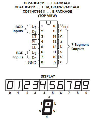
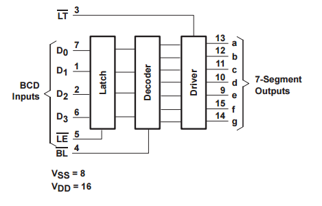
Figure 5. The 4511 BCD to 7-segment latch / decoder / driver.
By using a latch / decoder / driver such as the 4511 decoder (datasheet) the designer has many more options for display. By using the BCD decoder only four lines are required to drive the seven segments.
Figure 6. 4511 function diagram.
BL: blanking. Pull low to turn all segments off. Display: blank.
LT: lamp-test. Pull low to turn all segments on. Display: ‘8’.
LE: latch enable. Pull low to read the inputs and pass through to the seven segment outputs. Pull high to latch the outputs.
Note that BCD values above ‘9’ are considered void and the display will be blank. This renders the 4511 unsuitable for hexadecimal display.
The 4511 can source or sink current for the displays. See the datasheet for ratings.
Flicker-free 7-segment display
Figure 6. By using a 4511 latch per display a flicker-free display is possible.
Figure 5 shows how to use a 4511 latch per digit. In this case the data for each digit is set up in turn on D0 to D3 and the digit’s /LE (latch enable) pin is pulled low. The seven-segment display will immediately update and will be latched when the /LE pin is pulled high again. This, for example, would allow the micro to handle other tasks without having to update the display until required. The D0 to D3 IO pins could even be used as inputs with suitable input resistors while the diplay update is not required.
Note that the display decimal points are not controlled by the 4511. This leaves the designer with several options:
No decimal point.
A fixed decimal point by wiring one of the DP pins to Vss.
Program controlled decimal point. This will require one extra controller output pin per decimal point.
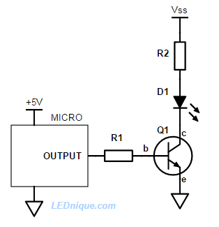
For various reasons it is often necessary to control LEDs supplied by a voltage higher than the micro-controller can supply or withstand. In these cases the most common solution is to use an NPN transistor as a switch or driver to buffer between the two parts of the circuit – the low-voltage control circuit and the high-voltage load circuit.
An NPN transistor can be used to act as a switch controlled by a low-voltage micro-controller switching a high voltage or high-current load.
When there is no current flowing into the base (b) of Q1 the transistor is off and no current flows from the collector (c) to the emitter (e). As we increase the current into the base of the transistor the transistor starts to turn on and its resistance falls allowing current to flow from Vss, through R2, D1 and Q1 to ground.
Small signal transistors have a “current gain” of 50 to 300. This means that for 0.1 mA into the base we should be able to get 5 to 30 mA to flow through the collector. The relationship is given by the equation \( I_C = h_{FE}I_B \) where \( I_C \) is the collector current, \( h_{FE} \) is the current gain and \( I_B \) the base current.
At first glance it seems that we could control the LED current to any value we wanted by controlling the base current. Unfortunately there is enough variation between transistors and the fact that this parameter is temperature dependent that this would not be a good reliable and repeatable design. (It might be OK for a one-off project provided you were confident you would never have to replace the transistor.)
Instead we inject more than enough current into the base to turn the transistor “hard” into saturation: the collector voltage drops as low as it can go – typically below 0.2 V.
Example 1 (NPN driver)
Our micro-controller output is a 5 V signal.
Vss is 12 V.
The LED, D1 requires 100 mA and will have a forward voltage of 2.8 V at that current.
Q1 has a \( h_{FE} \) of somewhere around 100.
R1
We want to ensure that the transistor saturates to give minimum voltage drop between the collector and emitter. In saturation we’ll assume that a current gain of 10 to 20 is likely. To guarantee saturation we should design for a base current of 5 to 10 mA. This will be fine for most micro-controllers (but always check the specification). The base voltage will rise to about 0.6 V when forward biased so the voltage across R1 will be 5 – 0.6 = 4.4 V. We can calculate (from Ohm’s Law) \( R_1 = \frac {V}{I} = \frac {4.4}{0.005} = 880\,\Omega \) and it would be half of that at 10 mA. We can go somewhere in-between with a 560 Ω or 680 Ω resistor.